(Hong Kong)

Product Summary
The LTC4352CDD creates a near-ideal diode using an external N-channel MOSFET. It replaces a high power Schottky diode and the associated heat sink, saving power and board area. The ideal diode function permits low loss power ORing and supply holdup applications. The LTC4352CDD regulates the forward voltage drop across the MOSFET to ensure smooth current transfer in diode-OR applications.
Parametrics
LTC4352CDD absolute maximum ratings: (1)VIN, SOURCE Voltages: –0.3V to 24V; (2)VCC Voltage: –0.3V to 7V; (3)OUT Voltage: –2V to 24V; (4)CPO, GATE Voltages: –0.3V to 30V; (5)CPO D.C. Current: 10mA; (6)UV, OV, REV Voltages: –0.3V to 24V; (7)FAULT, STATUS Voltages: 0.3V to 24V; (8)FAULT, STATUS Currents: 5mA; (9)Operating Ambient Temperature Range: 0℃ to 70℃; (10)Storage Temperature Range: –65℃ to 150℃; (11)Lead Temperature (Soldering, 10 sec): 300℃.
Features
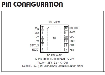
LTC4352CDD features: (1)Low Loss Replacement for Power Diode; (2)Controls N-Channel MOSFET; (3)0V to 18V Supply ORing or Holdup; (4)0.5μs Turn-On and Turn-Off Time; (5)Undervoltage and Overvoltage Protection; (6)Open MOSFET Detect; (7)Status and Fault Outputs; (8)Hot Swappable; (9)Reverse Current Enable Input; (10)12-Pin MSOP and DFN (3mm × 3mm) Packages.
Diagrams
| Image | Part No | Mfg | Description |  |
Pricing (USD) |
Quantity | ||||||||||
|---|---|---|---|---|---|---|---|---|---|---|---|---|---|---|---|---|
 |
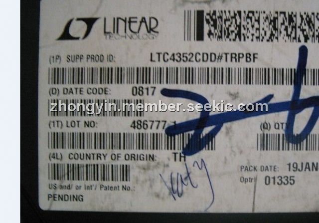
 LTC4352CDD#PBF |
|
IC IDEAL DIODE CNTRL 12-DFN |
Data Sheet |
|
|
||||||||||
|
LTC4352CDD#TRPBF |
|
IC IDEAL DIODE CNTRL 12-DFN |
Data Sheet |
|
|
||||||||||